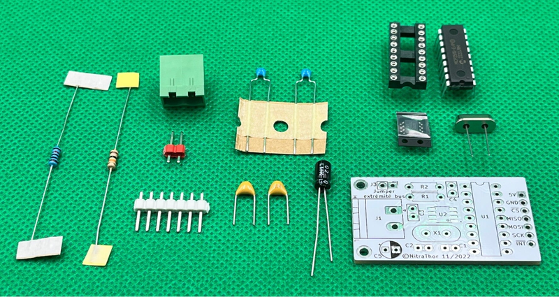
IBC - Network CAN bus communication interface card
For once, the IBC (CAN Bus Interface) card is a replica of an existing circuit with a few adaptations. This card will be used in all the modules of the automated network management and will allow inter-module communication.
If you are unfamiliar with the CAN bus, you can start by consulting the summary sheet dedicated to this protocol.
IBC Card Features
This small CAN interface card retains the same characteristics and perfect compatibility with commercial ones :
- Circuit board dimensions L 44 x W 26 mm ;
- 5V DC power supply ;
- Piloting carried out via the SPI protocol (integrated in the microcontrollers) ;
- Communication speed up to 1Mb/s ;
- Connection to the CAN bus by twisted pair ;
- Standby current: 1µA ;
- Working current: 5mA.
Maturity :
Interface board progress
Version 1.0
First version of the CAN card.
Its operation is fully validated. There are still a few corrections to be made in terms of component layout and footprint spacing.
The CAN bus connection terminal must also be modified in order to provide a connector without clamping screws at the PCB level. Indeed, there should be no space constraint above the card when it is installed in the final assembly.
Version 1.1
The CAN interface board is completely finalized and all anomalies have been corrected in this release.
The new terminal block allows connection to the CAN bus without technical intervention on the board (the twisted pair connection is made on the socket).
Necessary material (version 1.1)
| Description | Quantité | Référence PCB |
|---|---|---|
| Capacitor 22pF | 2 | C1, C2 |
| Capacitor 100nF | 2 | C3, C4 |
| Capacitor 10µF | 1 | C5 |
| CAN bus connection terminal block | 1 | J1 |
| Right pin header | 9 | J2, J3 |
| Resistor 10K | 1 | R1 |
| Resistor 120 ohms | 1 | R2 |
| 18-pin IC socket | 1 | U1 |
| MCP2515 | 1 | U1 |
| TJA1050T SMT | 1 | U2 |
| Quartz 8.000MHz | 1 | X1 |
Electronic diagram (version 1.1)
The order of the pins of the SPI connector is identical to that of commercial cards. The IBC interface card is perfectly compatible with its big sisters who know how to communicate with it. It is therefore possible to combine the IBC card with commercial CAN interface cards.
Functioning
Two integrated circuits make up this assembly :
- The MCP2515 contains all the management of the CAN protocol as well as an SPI interface for dialogue with the microcontroller. It has its own clock clocked at 8 MHz (X1, C1 and C2) ;
- The TJA1050 is used to manage physical exchanges with the CAN bus. It is thanks to this recent component that the number of possible nodes on the bus has been considerably increased (maximum 110 nodes).
Printed circuit board (version 1.1)
- The printed circuit has a ground plane on each side of the circuit in order to attenuate interference as much as possible.
- The two fixing holes on each side of the CAN socket make it possible to secure the interface card with the module which will house it and thus not exert any force on the SPI interface pins (J2) during connection / disconnection of the twisted pair.
Realization of the printed circuit
The zip file opposite contains :
- All assembly description files in gerber format (gbr extension) ;
- The drilling file (extension drl).
This compressed file can be used directly if you order the production of printed circuits from a service provider (see the tutorial "Have your PCB made").
Installation of components
Since it is up to you to make the CAN communication card and your bus will only necessarily have two loop-back resistors, you can therefore create two complete cards and for all the others, save the 120 ohm resistor and jumper pins. In this configuration, the only constraint will be to modify the position of the loopback card if you extend the CAN bus. (Which doesn't happen every day...)
Placing the components on the board does not pose any particular problem. if not the CMS component for which it is necessary to be meticulous.
The order of implementation is always the same. We start with the smallest component and end with the largest :
- Start with the TJA1050 (Be careful to correctly position pin 1 on the point of the U2 footprint on the PCB);
- The two resistors;
- Quartz;
- Non-polarized capacitors;
- The integrated circuit support (18 pins);
- The J2 and J3 connection pins (The SPI J2 connector is soldered on the underside);
- The polarized capacitor;
- Finish with the CAN bus connection terminal block.
You will need to make an IBC card for each electronic module of your network connected to the CAN bus... To your soldering irons !
Your email address will not be published. Mandatory fields are marked with *.


Comments
Add comment